一、 本期重点:
Doi:10.1364/ PRJ.3.000015
内容介绍:
本文第一次提出了基于多模干涉反射镜的片上锁模激光器。它不需要解理面来形成反馈,从而可以工作在芯片的任何位置。通过提供的连续光脉冲信号,可以实现芯片级的光信号处理(调制,滤波,脉冲倍频等)。芯片基于标准的InP基有源无源集成工艺,是信了基频的锁模运转。
图1 (a)两种类型的多模干涉反射镜结构及(b) 两种注入锁定激光器的结构
图2 两种使用多模干涉反射镜的锁模激光器结构,饱和吸收区工作在不同的位置
图3 实验装置图
doi: 10.1364/OPTICA.2.000076
published: 2014.1.21
内容介绍:
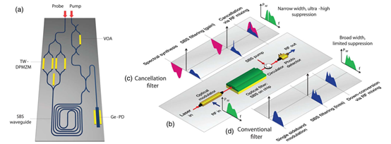
高选择性可重构微波滤波器在射频信号处理中有重要的应用。特别是微波光子滤波器,由于它相对电滤波器能够实现更灵活的重构以及频率调谐范围数量级上的提升。然而,目前的微波光子滤波器的一些关键参数如调谐范围、分辨率、抑制比等存在平衡,在集成器件中这些问题更严重,从而阻碍了更紧凑,更高性能滤波器的发展。这里我们首次实现了基于片上的具有超高抑制比,高分辨率的兆赫兹微波光子禁带滤波器,能实现0-30GHz的频率调谐。该实现基于光子芯片实现的超窄布里渊增益区以及光学谐振辅助RF信号相消的全新方法。该方法为无线通信提供了一种新的低功耗可重构集成微波光子滤波信号处理器的方案。
图1 基于受激布里渊散射的集成微波光子滤波器及其原理图
二、 简讯:
doi:10.1364/OE.23.014640
published: 2014.5.27
Abstract:
We propose, for the first time to our knowledge, a softwaredefined reconfigurable microwave photonics signal processor architecture that can be integrated on a chip and is capable of performing all the main functionalities by suitable programming of its control signals. The basic
configuration is presented and a thorough end-to-end design model derived that accounts for the performance of the overall processor taking into consideration the impact and interdependencies of both its photonic and RF parts. We demonstrate the model versatility by applying it to several relevant application examples.
doi: 10.1364/OPTICA.2.000366
published : 2015.4.9
Abstract:
The integration of ambient air plasmas as source and sensor in terahertz time-domain technique s allows spectral measurements covering the elusive terahertz gap (0.1– 10 THz), further increasing the impact of those scientific tools in the study of the four states of matter. In this article we describe the experimental study of the terahertz emission from a laser induced plasma of submillimeter size. The main direction of emission is almost orthogonal to the laser propagation direction, unlike that of elongated plasmas. We show that laser pulse energies lower than 1 μ J are sufficient to generate measurable terahertz pulses from ambient air. This significant decrease in the required laser energy will make plasma-based terahertz technique s more accessible to the scientific community.
doi: 10.1364/OE.23.013172
published : 2014.5.11
Abstract:
We report on a packaged prototype of a WDM photonic transceiver. It is an all-solid state hybrid assembly based on 130nm SOI photonic circuitry integrated with a 40nm CMOS VLSI driver. Our prototype supports eight tunable WDM channels operating at 10Gb/s, each capable of both transmitting and receiving data on the same chip. We discuss two options to close the link using the optical fiber or a waveguide bridge chip. We provide integration details and supporting link measurement data to describe packaged photonic module and its power efficient functionality with its on-chip power per channel averaging 1.3pJ/bit, excluding off-chip laser electrical power.
doi: 10.1364/OPTICA.2.000088
published:2014.1.26
Abstract:
Entanglement is a fundamental resource in quantum information processing. Several studies have explored the integration of sources of entangled states on a silicon chip, but the devices demonstrated so far require millimeter lengths and pump powers of the order of hundreds of milliwatts to produce an appreciable photon flux, hindering their scalability and dense integration. Micro-ring resonators have been shown to be efficient sources of photon pairs, but entangled state emission has never been proven in these devices. Here we report the first demonstration, to the best of our knowledge, of a micro-ring resonator capable of emitting time-energy entangled photons. We use a Franson experiment to show a violation of Bell’s inequality by more than seven standard deviations with an internal pair generation exceeding 107 Hz. The source is integrated on a silicon chip, operates at milliwatt and submilliwatt pump power, emits in the telecom band, and outputs into a photonic waveguide. These are all essential features of an entangled state emitter for a quantum photonic network.
供稿:胡志朋