
Doi: 10.1021/acsnano.5b00053
Published online: 2015.02.20
内容介绍:
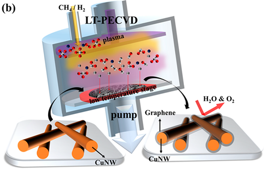
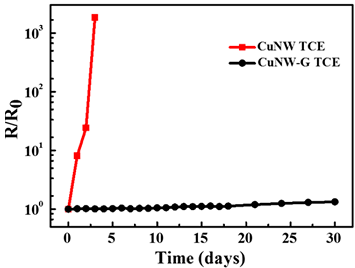
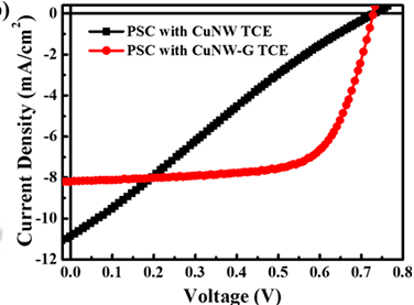
目前在光电子领域广泛应用的透明电极主要由ITO制成,但是,ITO也存在着易脆性,铟材料价格昂贵,高的工艺温度等问题,因而出现了替代性的新型透明电极,其中,随机银纳米线网络透明电极在光学和电学上都展现了优于ITO的特性,但是,Ag也是一种昂贵而稀有的材料,相比而言,铜的储量要丰富1000倍,价格只是银的1/80,并且导电性和银差不多,所以,铜纳米线(CuNW)透明电极也吸引了大批研究者的注意。
不过,CuNW在室温条件下暴露在空气中容易被氧化,导致其方块电阻急剧增加。为解决这一问题,作者使用PECVD首次在低达400℃的条件下在CuNW的表面包裹上石墨烯,利用石墨烯的不透气性和导电性,制作出了具有高度热和化学稳定性的透明电极,并将其应用到聚合物太阳能电池上。
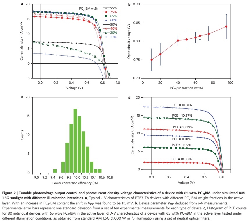
2、具有高效率和光电压的单结聚合物太阳能电池(Single-junction polymer solar cells with high efficiency and photovoltage)【Nature Photonics】
Doi: 10.1038/NPHOTON.2015.6
Published online: 9 FEBRUARY 2015
内容介绍:
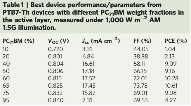
目前报道的单结聚合物太阳能电池的最高能量转换效率(PCE)在9%-10%,这主要受限于对太阳光谱相对较低的吸收重叠,为克服这一点,最直接的方法是采用窄带聚合物作为光收集材料,然而,用此概念制作出的太阳能电池尽管有100%的内部量子效率,PCE却还低于9%,这主要源于较低的开路电压(与最低未占据分子轨道(LUMO)和最高被占据分子轨道(HOMO)有关)。
本文中,作者合成出一种具有很深价带能级的高性能感光材料(PTB7-Th),并通过把其尾态密度(tail state density)减小到电子受体的导带之下,制作出了PCE超过10%的单结聚合物太阳能电池(认证效率9.94%)。他们对能带裁剪的控制是通过改变有源层的组分和混合物的结构次序实现的。
二、 简讯:
Doi: 10.1021/nn504969z
Published online: 2014.10.6
Abstract:
Recently, metal nanowires have received great research interests due to their potential as next-generation flexible transparent electrodes. While great efforts have been devoted to develop enabling nanowire electrodes, reduced contact resistance of the metal nanowires and improved electrical stability under continuous bias operation are key issues for practical applications. Here, we propose and demonstrate an approach through a low-cost, robust, room temperature and room atmosphere process to fabricate a conductive silver nano-network comprising silver nanowires and silver nanoparticles. To be more specific, silver nanoparticles are selectively grown and chemically integrated in situ at the junction where silver nanowires meet. The site-selective growth of silver nanoparticles is achieved by a plasmon-induced chemical reaction using a simple light source at very low optical power density. Compared to silver nanowire electrodes without chemical treatment, we observe tremendous conductivity improvement in our silver nano-networks, while the loss in optical transmission is negligible. Furthermore, the silver nano-networks exhibit superior electrical stability under continuous bias operation compared to silver nanowire electrodes formed by thermal annealing. Interestingly, our silver nano-network is readily peeled off in water, which can be easily transferred to other substratesand devices forversatile applications. We demonstrate thefeasibly transferrable silver conductive nano-network as thetop electrode inorganic solar cells. Consequently, the transparent and conductive silver nano-networks formed by our approach would be an excellent candidate for various applications in optoelectronics and electronics.
2.原子层厚度的砷烯和锑烯:半金属-半导体及间接-直接带隙跃迁(Atomically Thin Arsenene and Antimonene : Semimetal–Semiconductor and Indirect–Direct Band-Gap Transitions)
Doi: 10.1002/anie.201411246
Published: 2015.03.02
Abstract:
The typical two-dimensional (2D) semiconductors MoS2, MoSe2, WS2, WSe2 and black phosphorus have garnered tremendous interest for their unique electronic, optical, and chemical properties. However, all 2D semiconductors reported thus far feature band gaps that are smaller than 2.0 eV, which has greatly restricted their applications, especially in optoelectronic devices with photoresponse in the blue and UV range. Novel 2D mono-elemental semiconductors, namely monolayered arsenene and antimonene, with wide band gaps and high stability were now developed based on first-principles calculations. Interestingly, although As and Sb are typically semimetals in the bulk, they are transformed into indirect semiconductors with band gaps of 2.49 and 2.28 eV when thinned to one atomic layer. Significantly, under small biaxial strain, these materials were transformed from indirect into direct band-gap semiconductors. Such dramatic changes in the electronic structure could pave the way for transistors with high on/off ratios, optoelectronic devices working under blue or UV light, and mechanical sensors based on new 2D crystals.
Doi: 10.1038/NPHOTON.2015.9
Published:2015.02.09
Abstract:
Broadening the absorption bandwidth of polymer solar cells by incorporating multiple absorber donors into the bulk-heterojunction active layer is an attractive means of resolving the narrow absorption of organic semiconductors. However, this leads to a much more complicated system, and previous efforts have met with only limited success. Here, several dual-donor and multi-donor bulk-heterojunction polymer solar cells based on a pool of materials with different absorption ranges and preferred molecular structures were studied. The study shows clearly that compatible polymer donors can coexist harmoniously, but the mixing of incompatible polymers can lead to severe molecular disorder and limit device performance. These results provide guidance for the general use of multiple-donor bulk heterojunctions to overcome the absorption limitation and achieve both high performance and fabrication simplicity for organic solar cells.
Doi: 10.1002/anie.201412475
Published:2015.03.16
Abstract:
A new family of mechanochromic photonic-crystal fibers exhibits tunable structural colors under stretching. This novel mechanochromic fiber is prepared by depositing polymer microspheres onto a continuous aligned-carbon-nanotube sheet that has been wound on an elastic poly(dimethylsiloxane) fiber, followed by further embedding in poly(dimethylsiloxane). The color of the fiber can be tuned by varying the size and the center-to-center distance of the polymer spheres. It further experiences reversible and rapid multicolor changes during the stretch and release processes, for example, between red, green, and blue. Both the high sensitivity and stability were maintained after 1000 deformation cycles. These elastic photonic-crystal fibers were woven into patterns and smart fabrics for various display and sensing applications.
供稿人:寇鹏飞