一、本期重点:
Doi:10.1038/NPHOTON.2014.172
Published:17 August,2014
内容介绍:
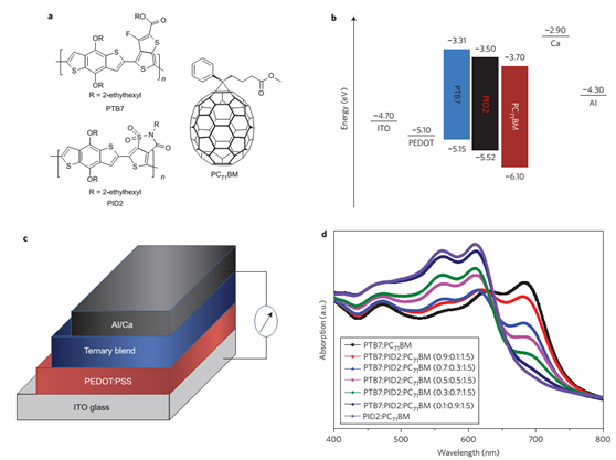
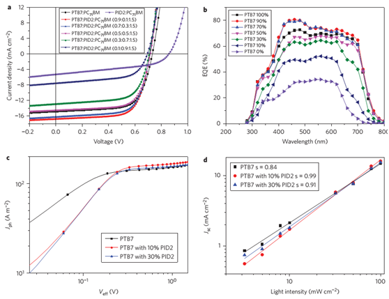
目前存在的大多数三元混合聚合物太阳电池(PSC)均以P3HT作为主要的施主聚合物,性能仍然较对应的二元PSC为差,并且在某些情况下,第三种组分会成为有源层内的复合中心或缺陷,进一步降低器件性能。
本文作者将一种新的有机物PID2(结构见下)作为额外的施主材料引入以PTB7:PC71BM为主体的二元混合物中,得到了转换率为8.22%(目前三元PSCs最高),短路电流16.8mA·cm-2,开路电压0.72V,FF为68.7%的太阳能电池,并研究了其性能随PID2含量的变化规律,得出了PID2:PTB7:PC71BM=0.9:0.1:1.5时性能最佳的结论。
作者根据分析试验认为,此器件具有较优良性能的原因是,改善的光收集,材料能级呈瀑布型以及优化的器件表面形貌。
Doi:10.1002/anie.201407688
Published:26 August,2014
内容介绍:
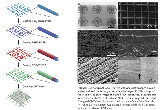
柔性电子织物被广泛认为是下一代电子器件很有前途的方向之一。目前存在的纤维形染料敏化太阳能电池(DSCs)由于采用液态电解液,需要封装,在薄、轻及可穿戴方面没有优势,以凝胶电解液替代时,其能量转化效率会大幅降低,并且效率随时间降低迅速,此外,以上两者仅弯折几次即不能工作,因而出现了纤维形聚合物太阳能电池(PSCs)。本文即提出一种有比较合理(1.08%)光伏性能的全固态、轻重量、柔性及可穿戴PSC。
其样品制作过程如下:①用Ti线制作Ti纺织品;②电化学氧化生长TiO2纳米管;③在TiO2纳米管表面引入TiO2纳米颗粒;④以dip-coating方法制作薄而连续的P3HT:PCBM和 PEDOT:PSS层;⑤制作对齐的碳纳米管电极层。
工作原理为:吸收光后,异质节产生激子,激子分离为空穴和电子;空穴被碳纳米管薄膜从PEDOT:PSS中抽取,电子通过TiO2传输到Ti织物阴极。由于修饰过的Ti织物两面均覆有聚合物有源层及对齐的碳纳米管薄膜,光从织物两面入射其转化效率基本相同。试验也表明该织物的抗弯曲性能很好。
二、 简讯:
Doi:10.1038/NNANO.2014.14
Published:2014.3.9
The limitations of the bulk semiconductors currently used in electronic devices—rigidity, heavy weight and high costs—have recently shifted the research efforts to two-dimensional atomic crystals such as graphene and atomically thin transition-metal dichalcogenides. These materials have thepotential to be produced at low cost and in large areas, whilemaintaining high material quality. These properties, as wellas their flexibility, make two-dimensional atomic crystals attractive for applications such as solar cells or display panels. The basic building blocks of optoelectronic devices are p–n junction diodes, but they have not yet been demonstrated in a two-dimensional material. Here, we report a p–n junction diode based on an electrostatically doped tungsten diselenide (WSe2) monolayer. We present applications as a photovoltaic solar cell, a photodiode and a light-emitting diode, and obtain light–power conversion and electroluminescence efficiencies of ∼0.5% and ∼0.1%, respectively. Given recent advances in the large-scale production of two dimensional crystals, we expect them to profoundly impact future developments in solar, lighting and display technologies.
Doi:10.1038/NPHOTON.2014.171
Published:2014.8.10
The unique and promising properties of semiconducting organometal halide perovskites have brought these materials to the forefront of solar energy research. Here, we present new insights into the excited-state properties of CH3NH3PbI3 thin films through femtosecond transient absorption spectroscopy measurements. The photo induced bleach recovery at 760 nm reveals that band-edge recombination follows second-order kinetics, indicating that the dominant relaxation pathway is via recombination of free electrons and holes. Additionally, charge accumulation in the perovskite films leads to an increase in the intrinsic bandgap that follows the Burstein–Moss band filling model. Both the recombination mechanism and the band-edge shift are studied as a function of the photogenerated carrier density and serve to elucidate the behaviour of charge carriers in hybrid perovskites. These results offer insights into the intrinsic photophysics of semiconducting organometal halide perovskites with direct implications for photovoltaic and optoelectronic applications.
Doi:10.1038/NPHOTON.2014.82
Abstract:
Lead-free solution-processed solid-state photovoltaic devices based on methylammonium tin iodide (CH3NH3SnI3) perovskite semiconductor as the light harvester are reported. Featuring an optical bandgap of 1.3 eV, the CH3NH3SnI3 perovskite material can be incorporated into devices with the organic hole-transport layer spiro-OMeTAD and show an absorption onset at 950 nm, which is significantly redshifted compared with the benchmark CH3NH3PbI3 counterpart (1.55 eV). Bandgap engineering was implemented by chemical substitution in the form of CH3NH3SnI3– xBrx solid solutions, which can be controllably tuned to cover much of the visible spectrum, thus enabling the realization of lead-free solar cells with an initial power conversion efficiency of 5.73% under simulated full sunlight. Further efficiency enhancements are expected following optimization and a better fundamental understanding of the internal electron dynamics and corresponding interfacial engineering. The reported CH3NH3SnI3– xBrx perovskite solar cells represent a step towards the realization of low-cost, environmentally friendly solid-state solar cells.
Doi:10.1002/pip.2378
Published:2013.4.27
Abstract:
InAs quantum dots (QDs) have been incorporated to bandgap engineer the (In)GaAs junction of (In)GaAs/Ge double-junctionsolar cells and InGaP/(In)GaAs/Ge triple-junction solar cells on 4-in. wafers. One sun AM0 current–voltage measurement showsconsistent performance across the wafer. Quantum efficiency analysis shows similar aforementioned bandgap performance ofbaseline and QD solar cells, whereas integrated sub-band gap current of 10 InAs QD layers shows a gain of 0.20 mA/cm2.Comparing QD double-junction solar cells and QD triple-junction solar cells to baseline structures shows that the (In)GaAsjunction has a Voc loss of 50 mV and the InGaP 70 mV. Transmission electron microscopy imaging does not reveal defectivematerial and shows a buried QD density of 1011 cm2, which is consistent with the density of QDs measured on the surface ofa test structure. Although slightly lower in efficiency, the QD solar cells have uniform performance across 4-in. wafers.
供稿:寇鹏飞