一、 本期重点:
DOI:10.1364/OE.22.012499
内容介绍:
本文提出了一种新型的利用纳米颗粒阵列(NPA)实现的光学谐振腔,并给出了利用其实现带宽可调谐的光滤波器的具体设计方法。利用NPA阵列和两端的玻璃平板实现谐振腔,并在纳米颗粒阵列两端填充介电常数可调的液晶物质,通过改变器件的物理特性、结构和材料特性,实现了从近红外到蓝光条件下的带宽调谐滤波器。该器件与偏振无关,且对光的入射角度不敏感,是很好的微纳可调谐光滤波器。
图1 (a)基于NPA的带宽可调谐光滤波器结构原理图(b)NPA平板及其等效电路(c)两种不同波长范围下的透射系数与反射系数
doi:10.1038
published:2014.2
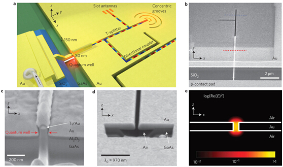
内容介绍:
电子和光子器件的小型化极大地促进了信息处理和传输的发展。等离子体能够突破衍射极限,从而实现微纳光线路。微纳光器件下一步的发展就是利用能够利用微纳光电路来驱动集成微纳光源。本文第一次提出了一种横截面仅0.016λ2电注入的等离子体LED与深亚波长等离子体刻蚀槽波导的单片集成器件,并从实验上给出了利用其实现空间路由,分支,自由空间耦合和定向耦合的实验结果。尽管电光转换效率很低,但它打开了全新的量子等离子体电路,微纳传感元件以及高速单模发射微纳光源的大门。
(a) 集成电驱动光子微纳电路原理图,包括刻蚀槽波导器件,两个微纳分支器,一个定向耦
合器和一个刻蚀槽天线 (b)微纳LED和刻蚀槽波导T型分支器的SEM图(c) 微纳LED SEM图 (d)悬浮刻蚀槽波导SEM图 (e)刻蚀槽波导耦合模式
二、 简讯:
doi:10.1364/OL.39.003204
published:2014.1.1
Abstract:
In this Letter, plasmonic sectoral horn nanoantennas working at near-infrared wavelength (1550 nm) have beeninvestigated. We demonstrate that, although there are certain differences between the plasmonic and classical radiofrequency (RF) sectoral horn antennas, the plasmonic horns still possess a number of attractive features, like their RFcounterparts, such as tunable high directivities, simplicity in fabrication, and ease of coupling to waveguides. As aspecific application, we further show how to exploit these findings to optimize an optical wireless nanolink usingthe proposed horn nanoantennas, and obtain a 60-fold increase in the received power compared with the situation ofmatched dipole nanoantennas.
DOI:10.1364/OE.22.012379
Published:2014.5.19
Abstract:
We demonstrate both theoretically and experimentally that discrete diffraction resonance can be designed, fabricated, and successfully probed in functionalized – guidonic – coupled waveguide arrays. We evidence that double-barrier patterning of the coupling creates wavelengthindependent angular tunnel resonance in the transmitted and the reflected intensity of light beams freely propagating in the plane of the array. Transmission peaks obtained are associated with resonant excitation of the engineered array bound supermodes of the functionalized array, in agreement with accurate and practical numerical modeling based on extended coupled-mode theory. The linear operation of the guidonic resonant tunneling double barrier makes up an original resonator for discrete photonics, suitable for all-optical control of light.
DOI:10.1364/OE.22.011456
Published:2014.5.19
Abstract:
Simultaneous regeneration of four high-speed (160 Gbit/s) wavelength-division multiplexed (WDM) and polarization-division multiplexed (PDM) signals in a singlehighly nonlinear fiber (HNLF) is demonstrated. The regeneration operation is based on four-wave mixing in HNLF, where the degraded data signals are applied as the pump. As a result, the noise on both ‘0’ and ‘1’ levels can be suppressed simultaneously in our scheme. The stimulated Brillouin scattering (SBS) from the continuous wave (CW) is suppressed by cross-phase modulation (XPM) from the data pump, relieving the requirement of external phase modulation of the CW light. Mitigation of the inter-channel nonlinearities is achieved mainly through an inter-channel 0.5 bit slot time delay. Bidirectional propagation is also applied to relieve the inter-channel four-wave mixing. The multi-channel regeneration performance is validated by bit-error rate (BER) measurements. The receiver powers at the BER of 10−9are improved by 1.9 dB, 1.8 dB, 1.6 dB and 1.5 dB for the four data channels, respectively.
doi:10.1364/OL.39.003106
published:2014.1.1
Abstract:
On-chip, high-power, erbium-doped distributed feedback lasers are demonstrated in a CMOS-compatible fabrication flow. The laser cavities consist of silicon nitride waveguide and grating features, defined by wafer-scale immersion lithography and an erbium-doped aluminum oxide layer deposited as the final step in the fabrication process. The large mode size lasers demonstrate single-mode continuous wave operation with a maximum output power of 75 mW without any thermal damage. The laser output power does not saturate at high pump intensities and is, therefore, capable of delivering even higher on-chip signals if a stronger pump is utilized. The amplitude noise of the laser is investigated and the laser is shown to be stable and free from self-pulsing when the pump power is sufficiently above threshold.
供稿:胡志朋