
一、 本期重点:
1.通过对纤锌矿砷化镓纳米线施加轴向力引发其直接带隙与伪直接带隙相互转换(Inducing a direct-to-pseudodirect bandgap transition in wurtzite GaAs nanowires withuniaxialstress)【Nature Communications】
Doi: 10.1038/ncomms4655
Published : 2014.4.10
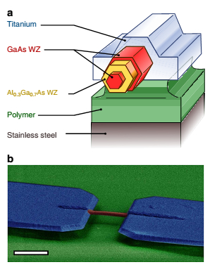
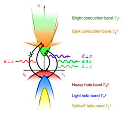
半导体材料直接与间接带隙(或者伪直接带隙)结构的相互转换将使新的光电应用成为可能,然而这往往需要较大的各向异性力。本文作者通过施加较小的轴向力引发纤锌矿GaAs纳米线的带隙结构在直接带隙与伪直接带隙之间可逆转换,使得其发光性能在开关之间切换。轴向拉伸时,纤锌矿GaAs为直接带隙,可作为发光材料;轴向压缩时,纤锌矿GaAs为伪直接带隙,可用于制作光电探测器。
他们试验用器件结构如下左图所示,使用沿c轴生长的GaAs-AlGaAs-GaAs单纳米线,用Ti固定到柔性衬底上,通过柔性衬底的不同弯曲方向实现对纳米线轴向的拉伸或压缩,再分别测量不同拉伸和压缩条件下的光致发光谱(PL)和拉曼谱。通过PL的可逆淬灭,他们第一次观察到了直接和伪直接带隙之间的转换,并分析了相应的能带变化情况。将拉曼散射谱作为参考标准,并且用k·p模型去拟合PL能量,他们还能得出闪锌矿砷化镓纳米线的所有能带结构参数。
Doi:10.1021/nn3013178
Published:2012.7.30
内容介绍:
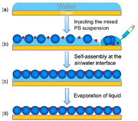
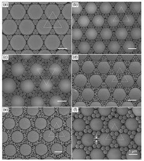
由于结构的多样性,在某些应用领域,二元胶质晶体(bCCs)相较于单尺寸胶质球有更多优点,然而对其结构的灵活设计及制作过程的精确控制仍然很困难。通过假设大小PS胶质球均存在于空气-水界面,本文作者建立了单层bCCs的相图及小球与大球尺寸比和数量比的范围图;以此为基础,可以设计和相对精确地控制制作特定结构的bCCs。
此外,他们在不用表面活性剂的情况下,用简单和精巧的方法制作出了有较大面积(>10cm2)的单层bCCs,具体见下左图。
二、 简讯:
doi:10.1021/nl404743j
published:2014.3.14
Abstract:
We report complementary metal−oxide−semiconductor (CMOS)-compatible integration of compound semiconductors on Si substrates. InAs and GaAs nanowires areselectively grown in vertical SiO2 nanotube templates fabricatedon Si substrates of varying crystallographic orientations, includingnanocrystalline Si. The nanowires investigated are epitaxiallygrown, single-crystalline, free from threading dislocations, andwith an orientation and dimension directly given by the shape ofthe template. GaAs nanowires exhibit stable photoluminescence atroom temperature, with a higher measured intensity when stillsurrounded by the template. Si−InAsheterojunction nanowiretunnel diodes were fabricated on Si(100) and are electricallycharacterized. The results indicate a high uniformity and scalability in the fabrication process.
doi:10.1038/nature13177
published:2014.4.10
The steady increase in control over individual quantum systemssupports the promotion of a quantum technology that could provide functionalities beyond those of any classical device. Two particularly promising applications have been explored during the pastdecade: photon-based quantum communication, which guaranteesunbreakable encryptionbut which still has to be scaled to high ratesover large distances, and quantum computation, which will fundamentally enhance computabilityif it can be scaled to a large number of quantum bits (qubits). It was realized early on that a hybridsystem of light qubits and matterqubitscould solve the scalabilityproblem of each field—that of communication by use of quantumrepeaters, and that of computation by use of an optical interconnectbetween smaller quantum processors. To this end, the developmentof a robust two-qubit gate that allows the linking of distant computational nodes is ‘‘a pressing challenge’’.Herewedemonstratesuchaquantum gate between the spin state of a single trapped atom and thepolarization state of an optical photon contained in a faint laser pulse.The gate mechanism presentedis deterministic and robust, and isexpected to be applicable to almost any matter qubit. It is based onreflection of the photonic qubit from a cavity that provides stronglight–matter coupling. To demonstrate its versatility, we use thequantum gate to create atom–photon, atom–photon–photon andphoton–photon entangled states from separable input states. Weexpect our experiment to enable various applications, including thegeneration of atomicand photoniccluster states and Schro ¨dingercat states, deterministic photonic Bell-state measurements,scalable quantum computationand quantum communication using aredundant quantum parity code.
doi: 10.1038/NPHOTON.2013.341
Thin-film photovoltaics play an important role in the quest forclean renewable energy. Recently, methylammonium leadhalide perovskites were identified as promising absorbers forsolar cells. In the three years since, the performance of perovskite-based solar cells has improved rapidly to reach efficienciesas high as 15%. To date, all high-efficiency perovskite solarcells reported make use of a (mesoscopic) metal oxide, suchas Al2O3,TiO2or ZrO2, which requires a high-temperature sintering process. Here, we show that methylammonium leadiodide perovskite layers, when sandwiched between two thinorganic charge-transporting layers, also lead to solar cells withhigh power-conversion efficiencies (12%). To ensure a highpurity, the perovskite layers were prepared by sublimation in ahigh-vacuum chamber. This simple planar device structure andthe room-temperature deposition processes are suitable formany conducting substrates, including plastic and textiles.
doi: 10.1038/NPHOTON.2013.238
published:2014.1.30
Abstract:
Finding higher efficiency schemes for electron–hole separation is of paramount importance for realizing more efficient conversion of solar energy in photovoltaic and photocatalytic devices. Plasmonic energy conversion has been proposed as a promising alternative to conventional electron–hole separation in semiconductor devices. This emerging method is based on the generation of hot electrons in plasmonic nanostructures through electromagnetic decay of surface plasmons. Here, the fundamentals of hot-electron generation, injection and regeneration are reviewed, with special attention paid to recent progress towards photovoltaic devices. This new energy-conversion method potentially offers high conversion efficiencies, while keeping fabrication costs low. However, several considerations regarding the materials, architectures and fabrication methods used need to be carefully evaluated to advance this field.
供稿:寇鹏飞