
一、 本期重点:
doi:10.1038/nature12237
内容介绍:
由于硅基光电子器件能够与CMOS工艺大规模集成,实现硅基的光电子集成器件一直是全光高速通信的发展方向,其中硅基的光调制器、滤波器、探测器、光开关及波分复用器件都已经非常成熟,但由于硅是一种间接带隙材料,实现硅激光器一直是实现全光路由一个难题。其中利用拉曼效应实现光放大是实现硅激光的途径之一。
本文利用光子晶体实现高品质因子的微腔,它通过在光子晶体波导的轴向一个很小的区域内引入不同周期的晶格常数,拉低了能带,实现了光子晶体中等效的p-i-n结,形成微谐振腔。它利用泵浦光和拉曼光在横模的两个方向上具有不同的就对称性,在材料生长上选择特定的晶相来制作光子晶体波导,实现了非常高的拉曼增益放大。同时,通过设计有源区的光子晶体结构,能够精确控制泵浦光和拉曼光的频率间隔,使泵浦光和拉曼光分别从奇模波导和耦模波导中输出。最终实现了非常高的Q值(1011,比之前报道的高4个数量级),同时尺寸不足10um,阈值功率低达1mW,为实现硅激光器和放大器的大规模集成实现提供了可能。
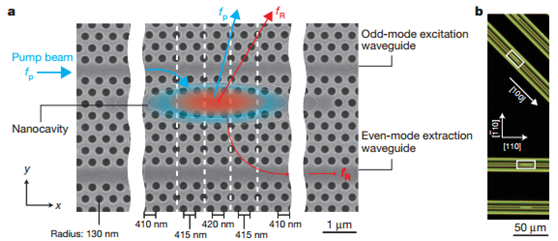
图1 (a)微腔拉曼硅激光机电镜结构图及(b)暗场显微图像(a为方框内的结构放大图)
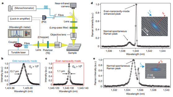
图2 (a)微腔激光器的光谱测试装置图(b,c)奇模和耦模的谐振谱(d)沿[100]方向微腔的拉曼光谱(e)沿[110]方向微腔的拉曼光谱
doi:10.1021/nl303510h
published:2013.1.16
内容介绍:
文章介绍了一种利用GaN纳米线实现片上光源及探测器的光互连器件,并介绍了它的制作方法、器件特性及纳米线光源与探测器之间的耦合特性。由于GaN能够很好地生长在硅材料上,因此能够实现硅基的光互连。对于两个轴向pn结结构的GaN纳米线,若电极分别放置在pn结的两端,就构成了一个LED,而如果电极均加在pn结的n侧,则构成了一个光电导器件,可以用来做光探测器。文章通过将这两个器件集成在同一衬底上,实现了片上光源与光探测器的集成,其中在GaN的LED引入电子阻挡层减少载流子的耗散。影响器件性能的主要因素是LED和探测器之间的耦合强度,取决于LED和探测器之间的距离。文章最终实现了功率为40nW的LED纳米线光源和10-7W/cm2的探测器灵敏度,为不同材料器件之间的光互连提供了可能。
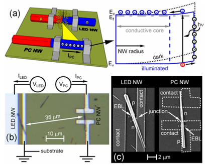
图1 耦合LED及光电导纳米线的 (a)工作原理图 (b)测试原理图 (c)SEM图
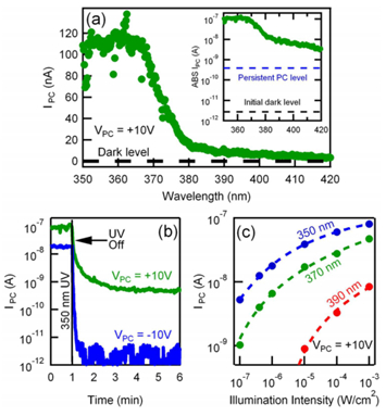
图2(a)光电流与激光器发射波长曲线图(b)光电导延时特性
(c)光电流与激光器光强曲线图
二、 简讯:
doi:10.1364/OE.21.011652
published:2013.5.6
Abstract:
We present 1-to-8 wavelength (de-)multiplexer devices based on a binary tree of cascaded Mach-Zehnder-like lattice filters, and manufactured using a 90 nm CMOS-integrated silicon photonics technology. We demonstrate that these devices combine a flat pass-band over more than 50% of the channel spacing with low insertion loss of less than 1.6 dB, and have a small device size of approximately 500 × 400 µm. This makes this type of filters well suited for application as WDM (de-)multiplexer in silicon photonics transceivers for optical data communication in large scale computer systems.
doi:10.1364/OL.38.000145
published:2013.1.8
Abstract:
Stimulated Raman scattering (SRS) microscopy allows label-free chemical imaging based on vibrational spectroscopy.Narrowband excitation with picosecond lasers creates the highest signal levels and enables imaging speeds up tovideo-rate, but it sacrifices chemical specificity in samples with overlapping bands compared to broadband (multiplex)excitation. We develop a rapidly tunable picosecond optical parametric oscillator with an electro-optical tunable Lyotfilter, and demonstrate multicolor SRS microscopy with synchronized line-by-line wavelength tuning to avoidspectral artifacts due to sample movement. We show sensitive imaging of three different kinds of polymer beadsand live HeLa cells with moving intracellular lipid droplets.
doi:10.1364/OL.38.000154
published:2013.1.9
Abstract:
We experimentally demonstrate a new optical filter design based on a vertically coupled photonic crystal (PhC)cavity and a bus waveguide monolithically integrated on the silicon-on-insulator platform. The use of a verticallycoupled waveguide gives flexibility in the choice of the waveguide material and dimensions, dramatically loweringthe insertion loss while achieving very high coupling efficiencies to wavelength scale resonators and thus allows thecreation of PhC-based optical filters with very high extinction ratio (>10dB).
doi:10.1364/OL.38.000374
published:2013.1.31
Abstract:
We have repeatedly and reproducibly switched a GaAs-AlAs planar microcavity operating in theoriginaltelecomband by exploiting the virtually instantaneous electronic Kerr effect. We achieve repetition times as fast as 300 fs,thereby breaking the terahertz modulation barrier. The rate of the switching in our experiments is only determinedby optics and not by material-related relaxation. Our results offer opportunities for fundamental studies of cavityquantum electrodynamics and optical information processing in the subpicosecond time scale.
供稿:胡志朋