
1.基于多空间视角的气溶胶3D分布还原(Multi sky-view 3D aerosol distribution recovery) 【OPTICS EXPRESS】
doi:10.1364/OE.21.025820
published:2013.10.22
内容介绍:
传统的大气遥感技术中,一般需要假定气溶胶是一维分布,本中提出了一种遥感探测大气中气溶胶3D分布的方法。这是一种层析成像技术,主要过程是利用多个可见光波段内成像的相机,在一个非常大的视场下对天空中的多个方向,多个位置进行成像。与其他层析像技术不同的是,这种层析成像方式很直接,因为其辐射光源是单向不受控制的太阳光,主要由离轴散射光线进行成像,不依靠线性模型,还提出了一个基于3D辐射的成像模型。对于数据反演,文中提出了一个新的数据采集系统和重建气溶胶分布的特殊算法。该方法是对与这个模型相适应的消光函数求导,得到一个隐函数梯度,求得最小消光函数最小值。最后通过蒙特卡罗统计方法仿真来验证模型的正确性。
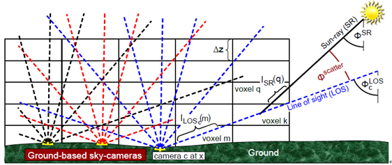
图1 利用地基相机探测立体大气示意图
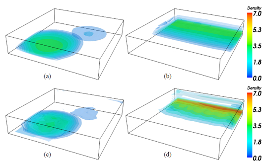
图2 仿真结果重现:颜色深浅代表气溶胶密度,单位是106/m3 (a)和(b)中单向散射作为输入(c)和(d)中蒙特卡罗图像作为输入
2.基于全息剪切镜头和空间傅里叶变换的白光横向剪切干涉仪(White light lateral shear interferometer with holographic shear lenses and spatial Fourier transform)【OPTICS LETTERS】
doi:10.1364/OL38.004896
pulished:2013.11.15
内容介绍:
横向剪切干涉仪因其结构简洁,功能强大,常被用来测量波前和折射率的改变。本文提出了一种利用白光照射全息光栅进行波前剪切的方法,由白光光谱中的某一特定波长光形成的空间载波条纹进行波前分析。这种方法的主要优势是其灵敏度可以通过两种方法来调节:一种是将全息平板换成全息光栅从而增加剪切,其次是通过选择衍射级次来选择短波波长,因为波长越短,灵敏度越高。本文在理论上和实验上对于白光的横向剪切干涉仪进行了分析。
实验发现,使用多重全息片可以更易于剪切和干涉。同时实验证实了白色光源的空间相干性可以通过聚焦透镜和针孔来加强。最后,由于衍射和多个透镜产生的光谱使得剪切干涉仪的灵敏度可以通过选择合适波长的光来调节。
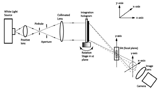
图1 基于集成全息的白光横向剪切干涉仪结构示意图,其剪切方向是y轴
二、简讯:
doi:10.1038/nphoton.2013.311
published:2013.11.24
Abstract:
The fundamental mechanism underlying photocurrent generation in carbon nanotubes has long been an open question. In photocurrent generation, the temperature of the photoexcited charge carriers determines the transport regime by which the electrons and holes are conducted through the nanotube. Here, we identify two different photocurrent mechanisms for metallic and semiconducting carbon nanotube devices with induced p–n junctions. Our photocurrent measurements as a function of charge carrier doping demonstrate a thermal origin for metallic nanotubes, where photo-excited hot carriers give rise to a current. For semiconducting nanotubes we demonstrate a photovoltaic mechanism, where a built-in electric field results in electron–hole separation. Our results provide an understanding of the photoresponse in carbon nanotubes, which is not only of fundamental interest but also of importance for designing carbon-based, high-efficiency photodetectors and energy-harvesting devices.
doi:10.1038/nphoton.2013.309
Published:2013.11.24
Abstract:
Raman spectroscopy uses visible light to acquire vibrational fingerprints of molecules, thus making it a powerful tool for chemical analysis in a wide range of media. However, its potential for optical imaging at high resolution is severely limited by the fact that the Raman effect is weak. Here, we report the discovery of a giant Raman scattering effect from encapsulated and aggregated dye molecules inside single-walled carbon nanotubes. Measurements performed on rod-like dyes such as α-sexithiophene and β-carotene, assembled inside single-walled carbon nanotubes as highly polarizable J-aggregates, indicate a resonant Raman cross-section of (3 ± 2) × 10−21 cm2 sr−1, which is well above the cross-section required for detecting individual aggregates at the highest optical resolution. Free from fluorescence background and photobleaching, this giant Raman effect allows the realization of a library of functionalized nanoprobe labels for Raman imaging with robust detection using multispectral analysis.
doi:10.1364/OL.38.005446
Published:2013.12.13
Abstract:
Multiwavelength shearing interferometry, a full-field, real-time, and vibration-insensitive method with enhanced accuracy, is proposed. Theoretically, the more wavelengths that are used for shearing interferometers, the higher the precision that can be achieved in the measurement of slopes, curvatures, and the shapes of reflective surfaces. A spherical mirror with specified curvature radius is used to calibrate this method, and then the nonuniform deformation and shape of the TiNi film/Si substrate system are obtained experimentally.
doi:10.1364/AO.52.008747
Publicshed:2013.12.16
Abstract:
The increasing scale of cryogenic detector arrays for submillimeter and millimeter wavelength astrophysics has led to the need for large aperture, high index of refraction, low loss, cryogenic refracting optics. Silicon with n=3.4, low loss, and high thermal conductivity is a nearly optimal material for these purposes but requires an antireflection (AR) coating with broad bandwidth, low loss, low reflectance, and a matched coefficient of thermal expansion. We present an AR coating for curved silicon optics comprised of subwavelength features cut into the lens surface with a custom three-axis silicon dicing saw. These features constitute a metamaterial that behaves as a simple dielectric coating. We have fabricated silicon lenses as large as 33.4 cm in diameter with micromachined layers optimized for use between 125 and 165 GHz. Our design reduces average reflections to a few tenths of a percent for angles of incidence up to 30° with low cross polarization. We describe the design, tolerance, manufacture, and measurements of these coatings and present measurements of the optical properties of silicon at millimeter wavelengths at cryogenic and room temperatures. This coating and lens fabrication approach is applicable from centimeter to submillimeter wavelengths and can be used to fabricate coatings with greater than octave bandwidth.
供稿:罗敬