
From 30th November to 6th December, 2019, six doctoral students from IEEE branch of Optical Science and Engineering College led by Dr. Chen Rui went to Korean Advanced Institute of science and Technology (KAIST) and Seoul National University for one week’s exchange and interview activities under the support of College of Optical Science and engineering. During this period, the group visited Advanced Display and Nano Convergence Laboratory (ADNC) of KAIST college and Optical Engineering and Quantum Electronics Laboratory (OEQELAB) of Seoul National University. This visit not only carried out business exchanges among IEEE branches, but also strengthened the exchanges between Zhejiang University and the two famous universities through seminars, lecture lab visits and other rich academic activities, expanded the academic vision of doctoral students, exercised and improved their academic exchange ability.
The visit to the Korean Academy of science and technology
Korean Advanced Institute of science and Technology (한국과학기술원, KAIST), also known as Korean Academy of science and technology. Founded in 1971, it is a public research university located in Daejeon, South Korea. It is a member of the Pacific Rim University Alliance. On November 27, 2019, the 2020QS Asian university ranking was released, and the Korean Academy of science and technology ranked ninth. KAIST has international level education and research and development facilities, implements the bachelor's, master's and doctor's continuous reading system, adopts the talent training system combining teaching and scientific research, and cultivates a large number of senior talents with high theoretical knowledge and practical application ability, making important contributions to the technological and economic development of South Korea. Most of the graduates of the Institute have entered Korean large enterprises, research institutes, educational institutions and government agencies, with 90.3% of the employers' satisfaction.
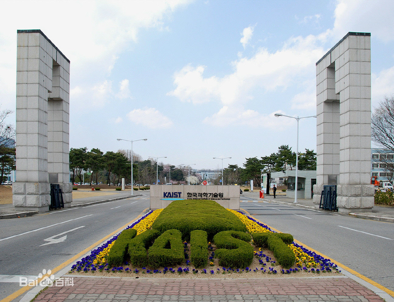
The gate of KAIST
On December 2, our group came to the Institute of Electrical Engineering of the Korean Academy of science and technology. We were received by Professor kyungsik Yu, who studied at Stanford University in the United States and worked in UC Berkeley. Mainly engaged in nano photonics, plasma optics, micro nano optical devices and semiconductor optoelectronic devices experimental and theoretical research. He has rich experience in the experimental fabrication and design of silicon-based and semiconductor metamaterials and plasmonic metasurface optoelectronic devices. Professor Yu first introduced the situation of KAIST University and its school of electronic engineering, and welcomed the students of the school of light to go to graduate school and visit for exchange. Professor Yu introduced the development background of Optoelectronics and silicon-based photonics in turn. His KAIST research group studied the processing and application of optoelectronic devices in silicon-based photonics, semiconductor photonics, optical array based on MEMS control, nano Photonics and other fields. Professor Yu's laboratory has advanced nano optical equipment such as femtosecond laser, high-precision optical lens, electronic amplifier, etc. in combination with the photolithography equipment of KAIST’s clean laboratory, a series of high-quality semiconductor and silicon-based optoelectronic devices with application prospects can be fabricated.
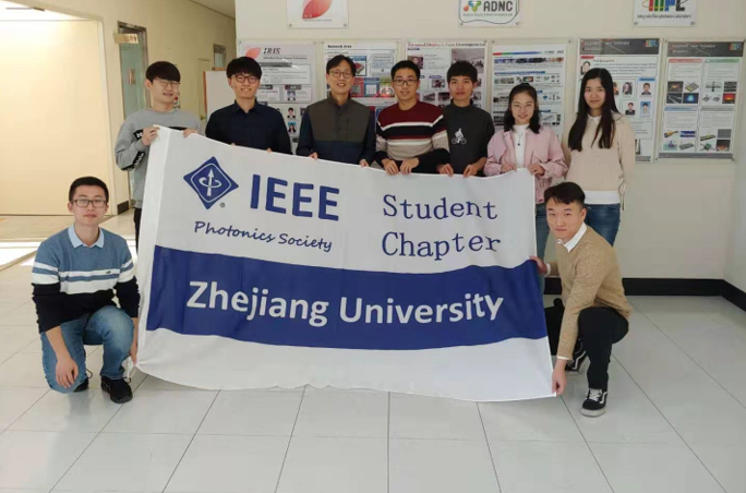
Photo with KAIST teachers and students
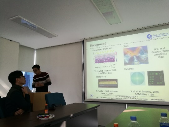
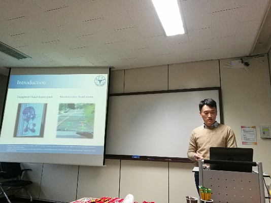
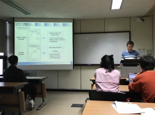
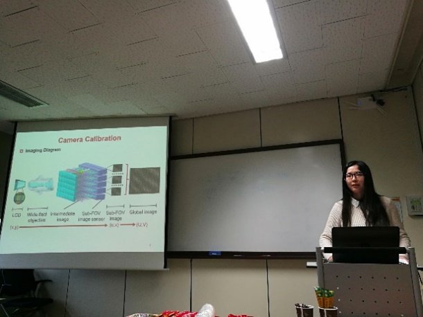
Then, the students of the visiting group and KAIST students gave interesting academic reports, respectively. The doctoral students of our group made reports on metasurface, super lens, holographic stereo imaging, high-speed three-dimensional imaging microscope and semiconductor nanowire laser, respectively. In the figure below, a Ph.D student from KAIST did optical doping on perovskite materials. Compared with traditional chemical doping and electrical methods, optical doping is more flexible and diverse. His purpose was to make a single photon source.
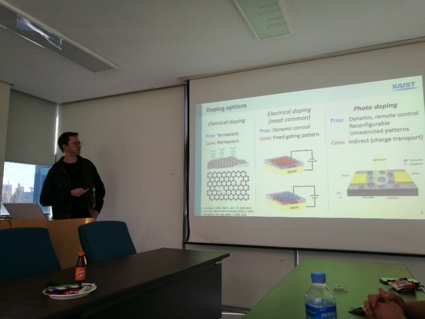
Reports from KAIST’s Ph.D student
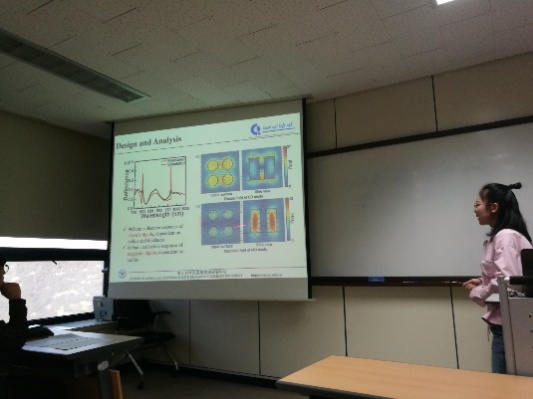
Reports from our group members
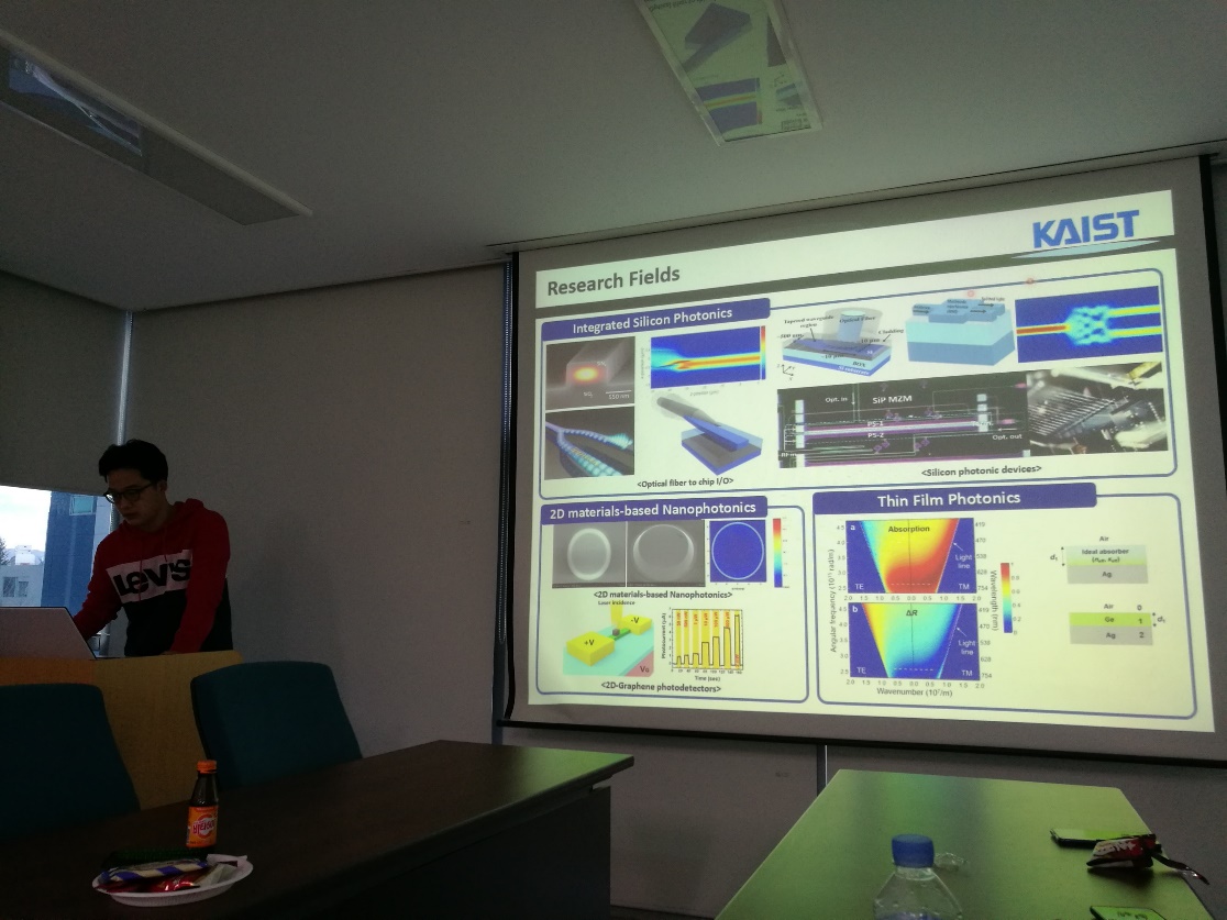
This is the person in charge of KAIST reception, Dr. Yoonhyuk Rah. He briefly introduced the main research directions of his laboratory. They mainly studied silicon-based integrated photonics and semiconductor photonics. Then they also carried out the processing and Application Research of nanowire photonics based on two-dimensional materials and thin-film optical optoelectronic devices.
Reports from Dr. Yoonhyuk Rah
Later, the visiting group visited yoonhyuk Rah's laboratory. Dr. Rah introduced the fabrication and coupling of silicon-based optical waveguide devices in their laboratory (top left, top right), and the devices of testing the optical and electrical characteristics in the cold chamber (bottom left). We also understand their whole processing and testing process, and deeply feel their systematic and meticulous spirit of doing things.

Yoonhyuk Rah's Lab
The visit to Seoul University
Seoul National University is located in guanyue District, Seoul special city. It is recognized as the highest institution in South Korea, and also one of the world-famous universities and the top research universities in Asia. After the initial words of the names of Seoul National University, Korea University and Yonsei University are merged, they are called "SKY" of Korean University.

The gate of Seoul National University
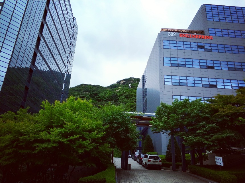
A corner of Engineering college
On the morning of 4th. December, the delegation arrived at Seoul National University to start the visit. We were warmly received by Dr. Jongwoo Hong, Later, Professor Byoungho Lee gave us a warm welcome report. His laboratory is Optical Engineering and Quantum Electronics Laboratory (OEQELAB). He said that he had held two meetings in Hangzhou before, and he liked Hangzhou and Zhejiang University very much. He also welcomed students from Zhejiang University to study or exchange visits with him. Then, Byoungho Lee briefly introduced the general situation of their laboratory. First, he introduced their laboratory in light field display, the work of holography near eye display and the innovative work of holography using metasurface in our research group were shared.
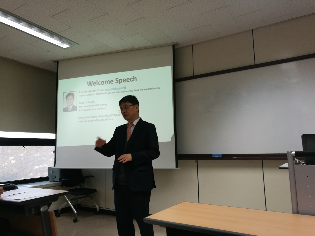
Welcome report by Professor Byungho Lee
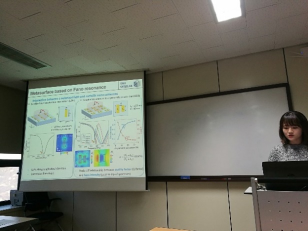
Next, Lee's research group arranged doctoral students, such as sang Eun Mun, Sun Je Kim and Changhyun Kim, to do "Fano resonant metasurface for narrowband light control" and " Dynamically tunable phase-change VO2 metagrating: ultra-broadband, efficient, and high contrast modulation of optical transmission " and " Multiwavelength achromatic metalens based on multiplexed multi-focal phase profile ", respectively. After that, the members of the our group also made our own reports, which aroused strong interest and heated discussion among the participants, and fully conducted useful exchanges.
Our group member and oeqelab students are making a report

Photo with OEQELAB teachers and students
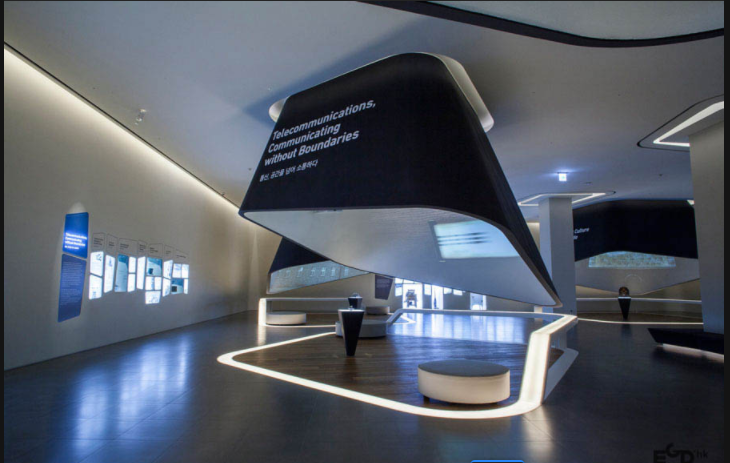
Later, the delegation visited the Samsung innovation Museum (SIM), which is located in the Samsung digital city of Suwon, South Korea. The museum was founded by Samsung Electronics, aiming to explore the past, present and future of the electronics industry.
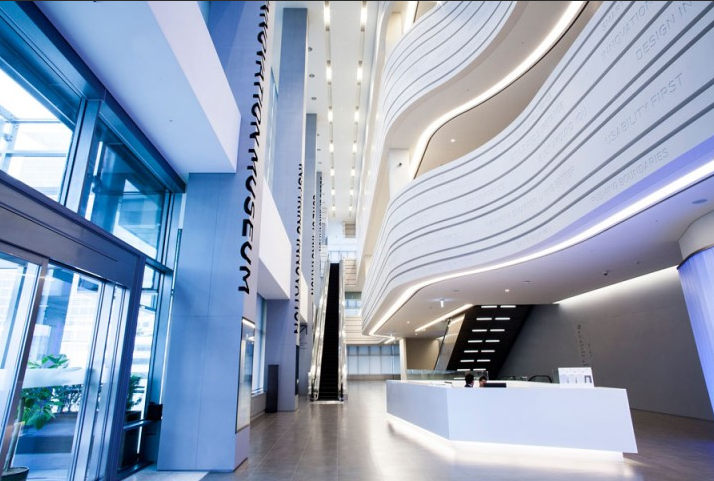
Samsung innovation Museum
We visited three parts of the museum, namely: The "inventor era" shows the origin of modern civilization and electronic industry. The collection includes the invention of Thomas Edison, Alexander Graham Bell, Michael Faraday and other famous inventors, as well as the development history of American Telephone and Telegraph Company, Siemens, Philips, Ge, NEC and other famous enterprises. "Enterprise innovation era" mainly displays the products of Samsung, apple, IBM, Sony and other companies in the display field. "Creation era" mainly displays the latest products of Samsung Electronics, B2B solutions, Samsung smart home and corporate vision.
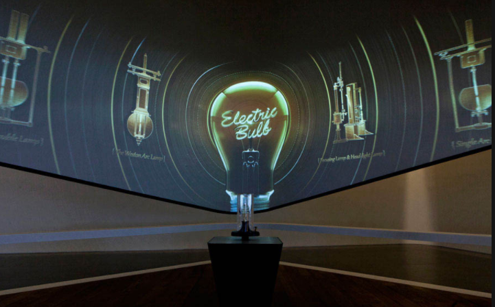
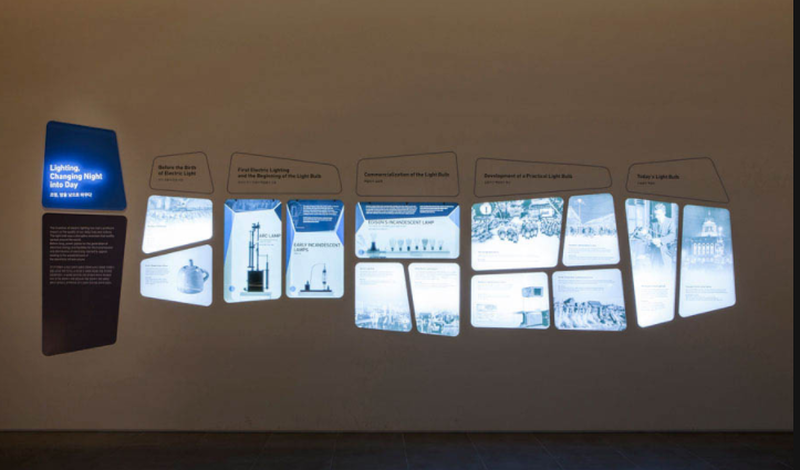
Samsung innovation Museum
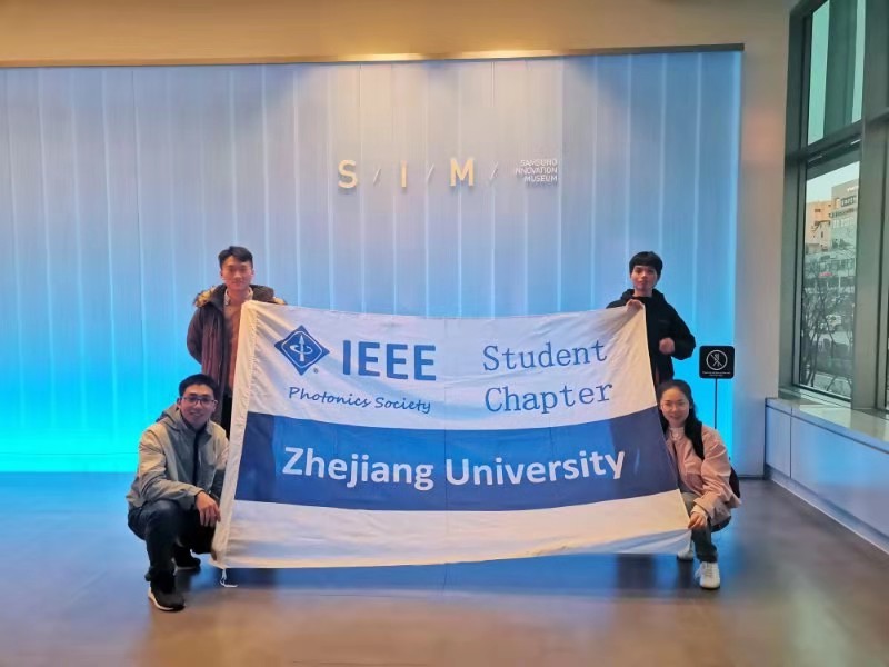

Group photo of the delegation at Samsung innovation Museum
Harvest of the visiting trip
The one-week visit ended soon, and the time of visit and exchange was short, but the harvest was great. Through the opportunity of this Korean academic exchange visit, we learned and experienced the research status and results of KAIST college and different research groups of Seoul University in Korea, understood their research directions and laboratory management methods, and experienced the first-class comprehensive in the world, entering the layout and development of the research center, we also felt the broad vision of the students there and their enthusiasm for scientific research and academic research. We found that the students there are especially hard-working, and the research was cutting-edge, which has left us a deep impression. It was a place we could learn and learn from in the future, and we hoped to communicate and cooperate with them more in the future. We also hoped that we could communicate and share with the excellent people around us in the future, so that we could become better people and contributed more to the society and the country!